|
|

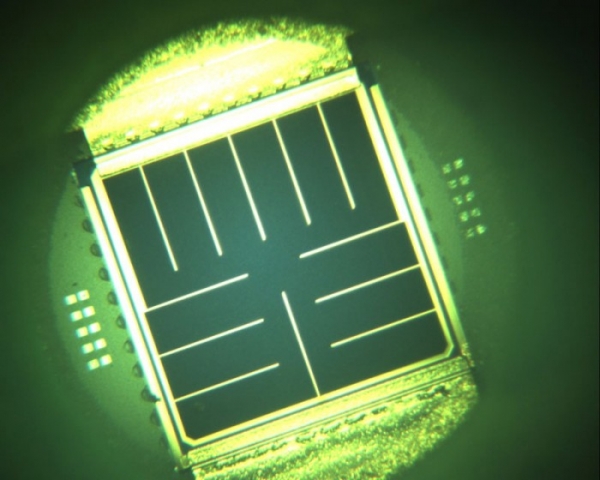 |
| NREL's state-of-the-art testing and characterization instruments scrutinize the quality and efficiency of solar cells, such as on this module made by Semprius. Image: NREL staff |
Most notable about the small size of the cell, is
that they occupy 1/1000 of the entire solar module
area, which is said to lead to an overall reduction
of the module cost. Furthermore, Semprius acknowledges
that by putting such large numbers of small cells
together, the heat is better distributed across the
cell’s structure, which can eliminate the need
for thermal management equipment.
Semprius states that it grows a temporary layer on
the original gallium-arsenide substrate and then
grows the multi-junction solar cell structure on
top of that layer.
Once the wafer is processed, the transfer printing process removes the cells from the gallium-arsenide substrate and transfers them to an interpose wafer. Semprius used its micro-transfer printing process to allow the micro-cells to be transferred from the growth substrate to a wafer. A large parallel process allows thousands of cells to be transferred at the same time, which additionally allows for the original substrate to be used repeatedly.
"We're using a completely different approach to what has been practiced," said Kanchan Ghosal, CPV applications engineering manager and the principal investigator for Semprius' PV Incubator Award. "This approach uses micro-cells and transfer printing to significantly reduce the use of materials in highly concentrated PV modules. And it provides a highly parallel method to manufacture the module, based on established microelectronics processes and equipment."
Semprius told the NREL that its low-cost approach can cut manufacturing expenses by 50%, a figure that the NREL noted Siemens acknowledged by taking a 16% stake in the company.
Updated: 2003/07/28